The Science Behind Our
Next-Generation Solar Platform
NovaSolix is developing a fundamentally new solar device architecture designed to capture far more of the sun’s energy than traditional photovoltaics. By harvesting light as electromagnetic waves rather than relying on bandgap-limited photon absorption, this approach opens the door to significantly higher efficiency, greater power density, and more reliable performance across real-world conditions.
How It Works
Carbon nanotube arrays unlock 4x density at half the cost – a step-change beyond silicon.
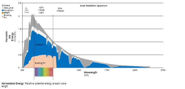
Our architecture uses nanoscale rectifying antennas—carbon-nanotube (CNT) structures sized to interact with the nanoscale wavelengths of sunlight. Unlike photovoltaic cells that rely on bandgap absorption, antenna structures convert electromagnetic radiation more efficiently by capturing sunlight as oscillating waves. These waves are then translated into electrical energy through ultra-fast tunnel diodes, a component NovaSolix has successfully fabricated at unprecedented switching speeds. Together, these nanoscale antennas and diodes enable a full-spectrum approach designed to harvest more energy across UV, visible, and infrared light.
Performance Capabilities of Our Architecture
NovaSolix’s rectenna architecture is designed to deliver substantially higher performance than traditional photovoltaic devices based on its theoretical capabilities. These performance characteristics demonstrate the potential for a solar device capable of producing more energy in more environments, supporting industries that require compact, high-output power solutions.
Limitations of Today’s Energy Technologies
Wind & Hydro
mature but geographically constrained; vulnerable to climate variability; limited utilization despite low LCOE.
Traditional Solar (PV)
narrow spectral absorption, intermittent output, and a practical efficiency ceiling defined by the Shockley–Queisser limit; density averages ~195 W/m².
Perovskites
promising efficiency but short lifespan and poor long-term stability.
Multi-Junction Cells
powerful but prohibitively expensive (> $100/W), preventing mass-market deployment.
Nuclear
carbon-free but slowed by high capital costs, regulatory hurdles, long build times (10+ years), and specialized workforce shortages.
What Our Solar Energy Technology Makes Possible
Captures ~2.5× broader spectrum range than PV, including UV and IR wavelengths.
Higher projected power density (~400 W/m²) compared to roughly 195 W/m² for standard silicon modules.
Operates more effectively in low-light and low-angle conditions, expanding usable daylight hours.
Compatible with global semiconductor supply chains, supporting faster production and scaling.
Lower material and production costs

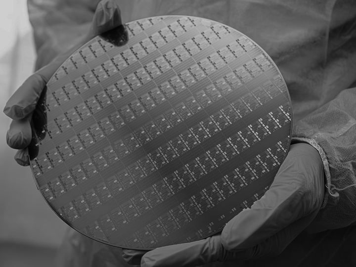
Manufacturing Compatibility for Rapid, Global Scale
NovaSolix’s new solar technology is engineered to integrate seamlessly into global semiconductor supply chains, enabling efficient and scalable production from the start. The device architecture is compatible with existing wafer production and etching tools, reducing barriers to adoption and allowing manufacturers to leverage equipment already used throughout the industry. With low-cost materials and a design that is scalable, the platform supports both early prototyping and future high-volume output.
Because the process produces more power for comparable manufacturing effort, shorter build cycles enable faster commercial rollout, positioning NovaSolix for rapid deployment once full-scale production begins.
Discover how our technology transforms industries that demand higher-output solar applications.